Microprocessor History and Generation of Microprocessor
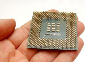
Fairchild semiconductors (founded in 1957) invented the first Integrated Circuit in 1959 that marked the microprocessor history. In 1968, Gordan Moore, Robert Noyce, and Andrew Grove resigned from the Fair child semiconductors and started their own company: Integrated Electronics (Intel). In 1971, the first microprocessor Intel 4004 was invented. A microprocessor is also known as a central processing unit in which numbers of peripherals’ are fabricated on a single chip. It has ALU (arithmetic and logic unit), a control unit, registers, bus systems, and a clock to perform computational tasks.
Architecture of Microprocessor
The microprocessor is a single IC package in which several useful functions are integrated and fabricated on a single silicon semiconductor chip. Its architecture consists of a central processing unit, memory modules, a system bus, and an input/output unit.
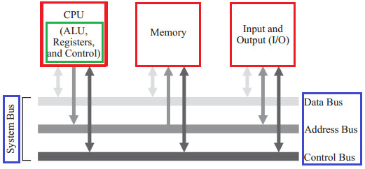
The system bus connects the various units to facilitate the exchange of information. It further consists of data, address, and control buses to perform data exchanging properly.
The Central processing unit consists of one or more arithmetic logic unit (ALU), registers, and control unit. Based on the registers also the generations of the microprocessor can be classified. A microprocessor consists of general-purpose and a special type of registers to execute instructions and to store the address or data while running the program. The ALU computes all arithmetic as well as logic operations on data and specifies the size of microprocessors like 16 bit or 32 bit.
The Memory unit holds the program as well as data and is divided into a processor, primary and secondary memory. The Input and output unit interfaces the I/O peripheral devices to the microprocessor for accepting and sending information.
Generation of Microprocessor
2nd Generation: This was the period from 1973 to 1978 in which very efficient 8-bit microprocessors were implemented like Motorola 6800 and 6801, INTEL-8085 and Zilog’s-Z80, which were among the most popular ones. Owing to their super fast speed, they were costly as they were based on NMOS technology fabrications.
3rd Generation: During this period 16-bit processors were created and designed using HMOS technology. From 1979 to 1980, INTEL 8086/80186/80286 and Motorola 68000 and 68010 were developed. Speeds of those processors were four times better than the 2nd generation processors.
4th Generation: From 1981 to 1995 this generation developed 32-bit microprocessors by using HCMOS fabrication. INTEL-80386 and Motorola’s 68020/68030 were the popular processors.
5th Generation: From 1995 to until now this generation has been bringing out high-performance and high-speed processors that make use of 64-bit processors. Such processors include Pentium, Celeron, Dual and Quad-core processors.
Thus, the microprocessor has evolved through all these generations, and the fifth-generation microprocessors represent an advancement in specifications. Therefore, some of the processors from the fifth generation of processors with their specifications are briefly explained below.
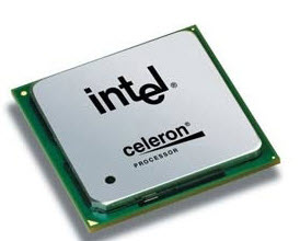
Intel Celeron
Intel Celeron is introduced in April 1998. It refers to a range of Intel’s X86 CPUs for value personal computer. It is based on Pentium 2 and can run on all IA-32 computer programs.
From the year 2000 to up to now, here is a brief history of Intel Celeron processors.
The year 2000 marked the introduction of the following processors:
- Jan 4-Intel Celeron Processor (533MHz)
- Feb14-Mobile Intel Celeron Processor (450, 500 MHz)
- June19-Low Voltage Mobile Intel Celeron Processor (500 MHz)
The year 2001 marked the introduction of the following processors:
- Jan 3-Intel Celeron Processor (800 MHz)
- Oct 2-Intel Celeron processor (1.2 GHz)
The year 2002 marked the introduction of the following processors:
- Jan 3-Intel Celeron Processor (1.30 GHz)
- Nov 20-Intel Celeron Processor (2.10, 2.20 GHz)
The year 2002 marked the introduction of the following processors:
- Jan 14: Mobile Intel Celeron processor (2 GHz)
- Low Voltage Mobile Intel Celeron Processor (866 MHz)
- Nov 12: Mobile Intel Celeron Processor (2.50GHz)
- Ultra-Low Voltage Mobile Intel Celeron Processor (800 MHz)
The year 2004-2007 marked the introduction of the following processors:
- Jan4, 2004: Intel Celeron M processor 320 and 310 (1.3, 1.2 GHz)
- July 20, 2004: Intel Celeron M processor Ultra Low voltage 353 (900 MHz)
- March- Intel Celeron M processor 430-450 (1.73-2.0 GHz)
- Nov 23: Intel Celeron D Processor 345 (3.06 GHz)
The year 2008 marked the introduction of the following processor:
- Jan 2008 Celeron Core 2 DUO (Allendale)
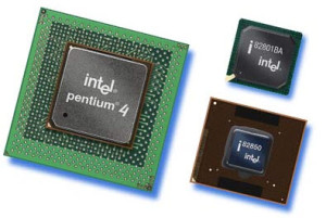
Pentium
Pentium was introduced on March 2, in 1993. Pentium succeeded the Intel 486; The 4 indicates the fourth generation microarchitecture in the microprocessor’s history. Pentium refers to an Intel’s single-core x 86 microprocessor, which is based on the fifth-generation micro-architecture. This processor’s name was derived from the Greek word Penta, means five.
The original Pentium processor was succeeded by the Pentium MMX in 1996. This processor has a data bus of 64 bits. A standard single transfer cycle can read or write up to 64 bits at a time. The Burst read and writes back cycles are supported by the Pentium processors. These cycles are used for cache operations and transfer 32 bytes (size of the Pentium cache line) in 4 clocks. All cache operations are burst cycles for the Pentium.
The year 2000 marked the introduction of the following processors:
- March 20: Intel Pentium III processor (866, 850MHz)
- March 8: Intel Pentium III processor (1GHz)
- Nov 20: Intel Pentium 4 Processor (1.50, 1.40GHz)
The year 2001 marked the introduction of the following processors:
- April 23: Pentium 4 Processor 1.7
- July 2: Pentium 4 Processor (1.80, 1.60GHz)
- Aug 27: Intel Pentium 4 Processor (2, 1.90 GHz)
The year 2002 marked the introduction of the following processors:
- Jan 7: Intel Pentium 4 processor (2.20, 2GHz)
- Jan 8: Intel Pentium III processor for servers (1.40 GHz)
- April 2, 2002: Intel Pentium 4 Processor (2.40, 2.20 GHz)
- Jan 21: Ultra Low Voltage Mobile Pentium III processor-M
- Low Voltage Mobile Pentium III processor (866, 850MHz)
- Nov 14, 2002: Intel Pentium 4 processor (3.06 GHz with HT technology)
The year 2003 marked the introduction of the following processors:
- Mobile Intel Pentium 4 Processor-M (2. 40 GHz)
- May 21: Intel Pentium 4 Processor with Hyper-Threading (2.80 C GHz, 2.60 C GHz, 2.40 C GHz)
- Nov 3: Intel Pentium 4 Processor Extreme Edition (3.20 GHz)
The year 20004 marked the introduction of the following processors:
- Feb 2, 2004: Intel Pentium 4 Processor (90nm) (3.40 GHz, 3.20 GHz, 3.0 GHz, 2.80 GHz)
- Intel Pentium 4 Processor Extreme Edition (0.13 micron) (3.40 GHz)
- April 7, 2004: Ultra Low Voltage Intel Pentium M Processor (1.10, 1.30 GHz)
- Nov 15, 2004: Intel Pentium 4 Processor Extreme Edition supporting HT Technology (3.46GHz)
The year 2005-06 marked the introduction of the following processors:
- Intel Pentium 4 Processor Extreme Edition supporting HT Technology (3.80GHz)
- April 2005: Intel Pentium Processor Extreme Edition 840 (3.20 GHz)
- The year 2007&08 marked the introduction of the following processors:
- Intel Pentium Processor Extreme Edition 955 (3.46 GHz)
- Intel Pentium Processor Extreme Edition 965 (3.73 GHz)
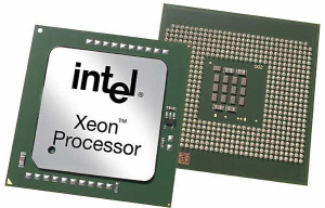
Xeon
Xeon processor is a 400 MHz Pentium processor from the Intel for use in workstations and enterprise servers. This processor is designed for multimedia applications, engineering graphics, Internet and large database servers.
A brief history of Xeon processors
The year 2000-2001 marked the introduction of the following processors:
- Jan 12: Intel Pentium III Xeon Processor (800 MegaHertz)
- Sep 25, 2001: Intel Xeon Processor (2 Giga Hertz)
- May 24: Intel Pentium III Xeon Processor (933 MegaHertz)
The year 2002-2004 marked the introduction of the following processors:
- Jan 09, 2002: Intel Xeon Processor (2.20 Giga Hertz)
- March 12, 2002: Intel Xeon Processor M (1.60 Giga Hertz)
- March 10, 2003: Intel Xeon Processor 3 GHz (400 MHz system bus)
- Nov 18: Intel Xeon Processor (2.80 Giga Hertz)
- Oct 6, 2003: Intel Xeon Processor (3.20 Giga Hertz)
- March 2, 2004: Intel Xeon Processor MP 3 GHz (4 MB L3 CACHE)
The year 2005-2008 marked the introduction of the following processors:
- March 2005: Intel Xeon Processor MP (2.666 -3.666 Giga Hertz)
- October 2005: Dual-Core Intel Xeon Processor (2.8 Giga Hertz)
- August 2006: Dual-Core Intel Xeon-7140M (3.33-3.40 Giga Hertz)
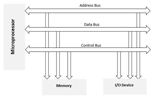
IO Interfacing
There are various communication devices like the keyboard, mouse, printer, etc. So, we need to interface the keyboard and other devices with the microprocessor by using latches and buffers. This type of interfacing is known as I/O interfacing.
Block Diagram of Memory and I/O Interfacing
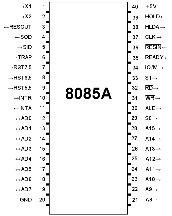
8085 Interfacing Pins
Following is the list of 8085 pins used for interfacing with other devices −
- A15 – A8 (Higher Address Bus)
- AD7 – AD0(Lower Address/Data Bus)
- ALE
- RD
- WR
- READY
Internal architecture of 8085 microprocessor
To work with microprocessor 8085, first we have to know the internal architecture of 8085 microprocessor. Internal architecture of 8085 microprocessor tells us the relation between different working blocks of 8085 microprocessor. Generally microprocessor consists of different working units those are
- Control unit: It control complete operations of microprocessor.
- ALU: It performs data processing function in respect of arithmetic and logical manner.
- Registers: It provide internal storage to CPU.
- Interrupts: It maintain priority of process.
- Internal data bus: It use to transfer data to appropriate place.
In bellow I shown the block diagram of internal architecture of 8085 microprocessor.

Now come to brief discussion on all individual units of internal architecture of 8085 microprocessor.
The ALU:
The ALU stands for arithmetic and logical unit. As name suggest all the arithmetic and logical operation of microprocessor done inside this unit. In addition to the arithmetic & logic circuits, the ALU includes the accumulator, which is part of every arithmetic & logic operation. Also, the ALU includes a temporary register used for holding data temporarily during the execution of the operation. This temporary register is not accessible by the programmer.
Registers:
Register is a very vital unit in internal architecture of 8085 microprocessor. These registers are used in different purpose. Mainly registers are three types
- General Purpose Registers
- Special Purpose Registers.
- Temporary Registers.
General Purpose Registers are by name B, C, D, E, H& L. All are 8 bit registers. It can be used singly Or can be used as 16 bit register pairs like BC, DE, HL. H & L can be used as a data pointer which holds memory address but it cannot make pair like BE, DC. So it should be in pair like BC, DE, HL.

Special Purpose Registers:
In 8085 microprocessor there have lots of special purpose register which have specific task. In bellow you find those special purpose register.
Accumulator (8 bit register):
Accumulator is very important register in 8085 microprocessor. It store 8 bit data in size. All arithmetic and logical operation done inside the accumulator and after execution store the result of an operation. It also used to store 8 bit data during I/O transfer.
Flag Register:
Flag is a brain of a microprocessor. It is an 8 bit register. It shows the status of the microprocessor before and after an operation. In 8085 microprocessor have five flags those are S (sign flag), Z (zero flag), AC (auxiliary carry flag), P (parity flag) & CY (carry flag).
Program Counter (PC):
Program counter is also a special purpose register. This is a register that is used to control the sequencing of the execution of instructions. This register always holds the address of the next instruction. Since it holds an address so it must be a 16 bits register.
Stack pointer:
As name suggested stack pointer used as an address pointer. The stack pointer is also a 16-bit register that is used to point into memory. The memory this register points to be a special area called the stack. The stack is an area of memory used to hold data that will be retrieved soon. The stack is usually accessed in a Last In First Out (LIFO) fashion.
8085 Microprocessor Pin Configuration
The 40 pins of the microprocessor can be divided into six groups such as address bus, data bus, control signals & status signals; power supply & frequency, externally started signals and serial input/output ports.
Address Bus (A8-A15)
The address bus pins are ranges from A8 to A15 and these are mainly applicable to the most considerable memory address bit.
Address Bus (or) Data Bus (AD0-AD7)
The address bus pins or data bus pins are ranges from AD0 to AD7, and these pins are applicable for LSB (least significant bits) of the address bus in the primary apparatus CLK cycle as well as employed as a data bus for second clock cycle & third clock cycle.
A CLK cycle can be designed as, the time in use among two oscillator’s nearby pulses, or simply it can refer to zero volts. Here the first clock is the primary transition of pulse ranges from 0V to 5V & then reaches back to 0V.
Address Latch Enable (ALE)
Basically, ALE assists in de-multiplexing the data bus as well as low order address. This will go high throughout the primary clock cycle as well as allows the address bits with low order. The address bus with low order is added for memory otherwise any exterior latch.
Status Signal (IO/M)
The status signal IO/M resolves whether the address is intended for memory or input/output. When the address is high then the address of the address bus is used for the devices of input/output devices. When the address is low then the address of the address bus is used for the memory.
Status Signals (S0-S1)
The status signals S0, S1 gives different functions as well as status based on their status.
- When the S0, S1 are 01 then the operation will be HALT.
- the S0, S1 is 10 then the operation will be WRITE
- When the S0, S1 is 10 then the operation will be READ
- When the S0, S1 are 11 then the operation will be FETCH
Active Low Signal (RD)
The RD is an energetic low signal and an operation is executed whenever the indication goes small, and it is used for controlling the microprocessor READ operation. When RD pin goes small then the 8085 microprocessor understands the information from I/O device or memory.
Active Low Signal (WR)
This is an energetic low signal, and it controls the microprocessor’s write operations. Whenever WR pin goes small, then the information will be written to the I/O device or memory.
READY
The READY pin is employed with the 8085 microprocessor for ensuring whether a device is set for accepting or transferring data. A device may be an A/D converter or LCD display, etc. These devices are associated with the 8085 microprocessor with the READY-pin. When this pin is high, the device is prepared for transferring the information, if it is not then the microprocessor stays until this pin goes high.
HOLD
The HOLD pin specifies when any device is demanding the employ of address as well as a data bus. The two devices are LCD as well as A/D converter. Assume that if A/D converter is employing the address bus as well as a data bus. When LCD desires the utilize of both the buses by providing HOLD signal, subsequently the microprocessor transmits the control signal toward the LCD after that the existing cycle will be ended. When the LCD procedure is over, then the control signal is transmitted reverse to A/D converter.
HLDA
This is the response signal of HOLD, and it specifies whether this signal is obtained or not obtained. After the implementation of HOLD demand, this signal will go low.
INTR
This is an interrupt signal, and the priority of this among the interrupt is low. This signal can be allowed or not allowed by the software. When INTR pin goes high then the 8085 microprocessor completes the instruction of current which is being executed and then recognizes the INTR signal and progresses it.
INTA
When the 8085 microprocessor gets an interrupt signal, then it should be recognized. This will be done by INTA. As a result, when the interrupt will be obtained then INTA will go high.
RST 5.5, RST 6.5, RST 7.5
These pins are the restart maskable interrupts or Vectored Interrupts, used to insert an inner restart function repeatedly. All these interrupts are maskable, they can be allowed or not allowed by using programs.
TRAP
Along with the 8085 microprocessor interrupts, TRAP is a non-maskable interrupt, and it doesn’t allow or stopped by a program. TRAP has the maximum precedence between the interrupts. The priority order from maximum to low includes TRAP, RST 5.5, RST 6.5, RST 7.5, and INTR.
RESET IN
RESET IN pin is used to reset the program counter toward zero and rearranges interrupt enable as well as HLDA flip flops (FFs). The central processing unit is detained in RST condition till this pin is high. But the registers as well as flags won’t get damaged apart from instruction register.
RST (RESET) OUT
RESET OUT pin specifies that the central processing unit has been rearranged with RST IN.
X1 X2
X1, X2 terminals that are associated with the exterior oscillator for generating the required as well as appropriate operation of a clock.
CLK
Sometimes it is compulsory to generate CLK o/PS from 8085 microprocessors so they can be used in favor of other peripherals or else other digital integrated circuits. This is offered with CLK pin. Its frequency is continually similar because the frequency at which the microprocessor works.
SID
This is a serial i/p data, and the information on this pin is uploaded into the 7th-bit of the accumulator while RIM (Read Interrupt Mask) instruction is performed. RIM verifies the interrupt whether it is covered or not covered.
SOD
This is the serial o/p data, and the data on this pin sends its output toward the 7th-bit of the accumulator whenever an instruction of SIM is performed.
VSS and VCC
VSS is a ground pin whereas Vcc is +5v pin. Therefore the 8085 pin diagram, as well as signals, are discussed in detail.
Thus, this is all about the 8085 microprocessor From the above information finally, we can conclude that the actual name of this processor is 8085A. This processor is an NMOS device and consists of thousands of transistors. Here is a question for you, what is the function of Level Triggered Interrupt in 8085 microprocessor?
Block Diagram of Intel 8086
The 8086 CPU is divided into two independent functional units:
- Bus Interface Unit (BIU)
- Execution Unit (EU)
Fig. 1: Block Diagram of Intel 8086

Features of 8086 Microprocessor:
- Intel 8086 was launched in 1978.
- It was the first 16-bit microprocessor.
- This microprocessor had major improvement over the execution speed of 8085.
- It is available as 40-pin Dual-Inline-Package (DIP).
- It is available in three versions:
- 8086 (5 MHz)
- 8086-2 (8 MHz)
- 8086-1 (10 MHz)
- It consists of 29,000 transistors.
Bus Interface Unit (BIU)
The function of BIU is to:
- Fetch the instruction or data from memory.
- Write the data to memory.
- Write the data to the port.
- Read data from the port.
Instruction Queue
- To increase the execution speed, BIU fetches as many as six instruction bytes ahead to time from memory.
- All six bytes are then held in first in first out 6 byte register called instruction queue.
- Then all bytes have to be given to EU one by one.
- This pre fetching operation of BIU may be in parallel with execution operation of EU, which improves the speed execution of the instruction.
Execution Unit (EU)
The functions of execution unit are:
- To tell BIU where to fetch the instructions or data from.
- To decode the instructions.
- To execute the instructions.
The EU contains the control circuitry to perform various internal operations. A decoder in EU decodes the instruction fetched memory to generate different internal or external control signals required to perform the operation. EU has 16-bit ALU, which can perform arithmetic and logical operations on 8-bit as well as 16-bit.
General Purpose Registers of 8086
These registers can be used as 8-bit registers individually or can be used as 16-bit in pair to have AX, BX, CX, and DX.
- AX Register: AX register is also known as accumulator register that stores operands for arithmetic operation like divided, rotate.
- BX Register: This register is mainly used as a base register. It holds the starting base location of a memory region within a data segment.
- CX Register: It is defined as a counter. It is primarily used in loop instruction to store loop counter.
- DX Register: DX register is used to contain I/O port address for I/O instruction.
Segment Registers
Additional registers called segment registers generate memory address when combined with other in the microprocessor.In 8086 microprocessor, memory is divided into 4 segments as follow:
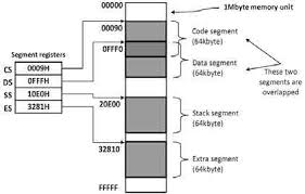
Fig. 2: Memory Segments of 8086
- Code Segment (CS): The CS register is used for addressing a memory location in the Code Segment of the memory, where the executable program is stored.
- Data Segment (DS): The DS contains most data used by program. Data are accessed in the Data Segment by an offset address or the content of other register that holds the offset address.
- Stack Segment (SS): SS defined the area of memory used for the stack.
- Extra Segment (ES): ES is additional data segment that is used by some of the string to hold the destination data.
Flag Registers of 8086
Flag register in EU is of 16-bit and is shown in fig. 3:
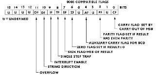
Fig. 3: Flag Register of 8086
Flags Register determines the current state of the processor. They are modified automatically by CPU after mathematical operations, this allows to determine the type of the result, and to determine conditions to transfer control to other parts of the program. 8086 has 9 flags and they are divided into two categories:
- Conditional Flags
- Control Flags
Conditional Flags
Conditional flags represent result of last arithmetic or logical instruction executed. Conditional flags are as follows:
- Carry Flag (CF): This flag indicates an overflow condition for unsigned integer arithmetic. It is also used in multiple-precision arithmetic.
- Auxiliary Flag (AF): If an operation performed in ALU generates a carry/barrow from lower nibble (i.e. D0 – D3) to upper nibble (i.e. D4 – D7), the AF flag is set i.e. carry given by D3 bit to D4 is AF flag. This is not a general-purpose flag, it is used internally by the processor to perform Binary to BCD conversion.
- Parity Flag (PF): This flag is used to indicate the parity of result. If lower order 8-bits of the result contains even number of 1’s, the Parity Flag is set and for odd number of 1’s, the Parity Flag is reset.
- Zero Flag (ZF): It is set; if the result of arithmetic or logical operation is zero else it is reset.
- Sign Flag (SF): In sign magnitude format the sign of number is indicated by MSB bit. If the result of operation is negative, sign flag is set.
- Overflow Flag (OF): It occurs when signed numbers are added or subtracted. An OF indicates that the result has exceeded the capacity of machine.
Control Flags
Control flags are set or reset deliberately to control the operations of the execution unit. Control flags are as follows:
- Trap Flag (TP):
- It is used for single step control.
- It allows user to execute one instruction of a program at a time for debugging.
- When trap flag is set, program can be run in single step mode.
- Interrupt Flag (IF):
- It is an interrupt enable/disable flag.
- If it is set, the maskable interrupt of 8086 is enabled and if it is reset, the interrupt is disabled.
- It can be set by executing instruction sit and can be cleared by executing CLI instruction.
- Direction Flag (DF):
- It is used in string operation.
- If it is set, string bytes are accessed from higher memory address to lower memory address.
- When it is reset, the string bytes are accessed from lower memory address to higher memory address.
