Flip Flop
Flip flop is a sequential circuit which generally samples its inputs and changes its outputs only at particular instants of time and not continuously. Flip flop is said to be edge sensitive or edge triggered rather than being level triggered like latches.
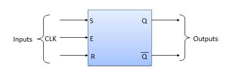
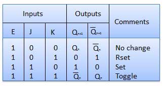
S-R Flip Flop
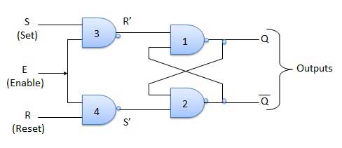
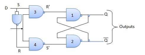
It is basically S-R latch using NAND gates with an additional enable input. It is also called as level triggered SR-FF. For this, circuit in output will take place if and only if the enable input (E) is made active. In short this circuit will operate as an S-R latch if E = 1 but there is no change in the output if E = 0.
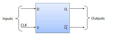
Block Diagram
Circuit Diagram
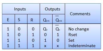
Truth Table
Operation
S.N.ConditionOperation1S = R = 0 : No change
If S = R = 0 then output of NAND gates 3 and 4 are forced to become 1.
Hence R’ and S’ both will be equal to 1. Since S’ and R’ are the input of the basic S-R latch using NAND gates, there will be no change in the state of outputs.2S = 0, R = 1, E = 1
Since S = 0, output of NAND-3 i.e. R’ = 1 and E = 1 the output of NAND-4 i.e. S’ = 0.
Hence Qn+1 = 0 and Qn+1bar = 1. This is reset condition.3S = 1, R = 0, E = 1
Output of NAND-3 i.e. R’ = 0 and output of NAND-4 i.e. S’ = 1.
Hence output of S-R NAND latch is Qn+1 = 1 and Qn+1 bar = 0. This is the reset condition.4S = 1, R = 1, E = 1
As S = 1, R = 1 and E = 1, the output of NAND gates 3 and 4 both are 0 i.e. S’ = R’ = 0.
Hence the Race condition will occur in the basic NAND latch.
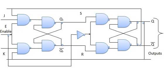
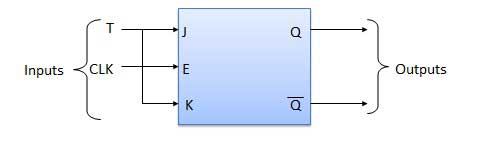
Master Slave JK Flip Flop
Master slave JK FF is a cascade of two S-R FF with feedback from the output of second to input of first. Master is a positive level triggered. But due to the presence of the inverter in the clock line, the slave will respond to the negative level. Hence when the clock = 1 (positive level) the master is active and the slave is inactive. Whereas when clock = 0 (low level) the slave is active and master is inactive.
Circuit Diagram
Truth Table
Operation
S.N.ConditionOperation1J = K = 0 (No change)
When clock = 0, the slave becomes active and master is inactive. But since the S and R inputs have not changed, the slave outputs will also remain unchanged. Therefore outputs will not change if J = K =0.2J = 0 and K = 1 (Reset)
Clock = 1 − Master active, slave inactive. Therefore outputs of the master become Q1 = 0 and Q1 bar = 1. That means S = 0 and R =1.
Clock = 0 − Slave active, master inactive. Therefore outputs of the slave become Q = 0 and Q bar = 1.
Again clock = 1 − Master active, slave inactive. Therefore even with the changed outputs Q = 0 and Q bar = 1 fed back to master, its output will be Q1 = 0 and Q1 bar = 1. That means S = 0 and R = 1.
Hence with clock = 0 and slave becoming active the outputs of slave will remain Q = 0 and Q bar = 1. Thus we get a stable output from the Master slave.3J = 1 and K = 0 (Set)
Clock = 1 − Master active, slave inactive. Therefore outputs of the master become Q1 = 1 and Q1 bar = 0. That means S = 1 and R =0.
Clock = 0 − Slave active, master inactive. Therefore outputs of the slave become Q = 1 and Q bar = 0.
Again clock = 1 − then it can be shown that the outputs of the slave are stabilized to Q = 1 and Q bar = 0.4J = K = 1 (Toggle)
Clock = 1 − Master active, slave inactive. Outputs of master will toggle. So S and R also will be inverted.
Clock = 0 − Slave active, master inactive. Outputs of slave will toggle.
These changed output are returned back to the master inputs. But since clock = 0, the master is still inactive. So it does not respond to these changed outputs. This avoids the multiple toggling which leads to the race around condition. The master slave flip flop will avoid the race around condition.
Delay Flip Flop / D Flip Flop
Delay Flip Flop or D Flip Flop is the simple gated S-R latch with a NAND inverter connected between S and R inputs. It has only one input. The input data is appearing at the output after some time. Due to this data delay between i/p and o/p, it is called delay flip flop. S and R will be the complements of each other due to NAND inverter. Hence S = R = 0 or S = R = 1, these input condition will never appear. This problem is avoid by SR = 00 and SR = 1 conditions.
Block Diagram
Circuit Diagram
Truth Table
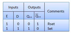
Operation
S.N.ConditionOperation1E = 0
Latch is disabled. Hence no change in output.2E = 1 and D = 0
If E = 1 and D = 0 then S = 0 and R = 1. Hence irrespective of the present state, the next state is Qn+1= 0 and Qn+1 bar = 1. This is the reset condition.3E = 1 and D = 1
If E = 1 and D = 1, then S = 1 and R = 0. This will set the latch and Qn+1 = 1 and Qn+1bar = 0 irrespective of the present state.
Toggle Flip Flop / T Flip Flop
Toggle flip flop is basically a JK flip flop with J and K terminals permanently connected together. It has only input denoted by T as shown in the Symbol Diagram. The symbol for positive edge triggered T flip flop is shown in the Block Diagram.
Symbol Diagram
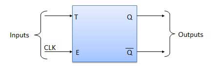
Block Diagram
Truth Table
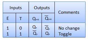
Operation
S.N.ConditionOperation1T = 0, J = K = 0The output Q and Q bar won’t change2T = 1, J = K = 1Output will toggle corresponding to every leading edge of clock signal.
Digital Registers
Flip-flop is a 1 bit memory cell which can be used for storing the digital data. To increase the storage capacity in terms of number of bits, we have to use a group of flip-flop. Such a group of flip-flop is known as a Register. The n-bit register will consist of n number of flip-flop and it is capable of storing an n-bit word.
The binary data in a register can be moved within the register from one flip-flop to another. The registers that allow such data transfers are called as shift registers. There are four mode of operations of a shift register.
- Serial Input Serial Output
- Serial Input Parallel Output
- Parallel Input Serial Output
- Parallel Input Parallel Output
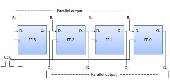
Serial Input Serial Output
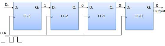
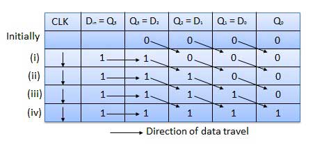
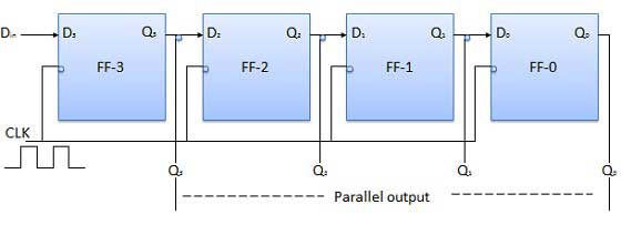
Let all the flip-flop be initially in the reset condition i.e. Q3 = Q2 = Q1 = Q0 = 0. If an entry of a four bit binary number 1 1 1 1 is made into the register, this number should be applied to Din bit with the LSB bit applied first. The D input of FF-3 i.e. D3 is connected to serial data input Din. Output of FF-3 i.e. Q3 is connected to the input of the next flip-flop i.e. D2 and so on.
Block Diagram
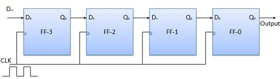
Operation
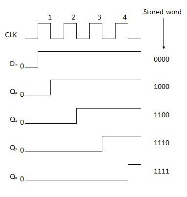
Before application of clock signal, let Q3 Q2 Q1 Q0= 0000 and apply LSB bit of the number to be entered to Din. So Din = D3 = 1. Apply the clock. On the first falling edge of clock, the FF-3 is set, and stored word in the register is Q3 Q2 Q1 Q0 = 1000.
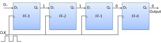
Apply the next bit to Din. So Din = 1. As soon as the next negative edge of the clock hits, FF-2 will set and the stored word change to Q3 Q2 Q1 Q0 = 1100.
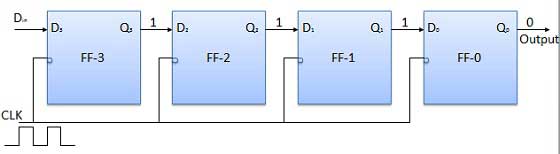
Apply the next bit to be stored i.e. 1 to Din. Apply the clock pulse. As soon as the third negative clock edge hits, FF-1 will be set and output will be modified to Q3 Q2 Q1 Q0 = 1110.
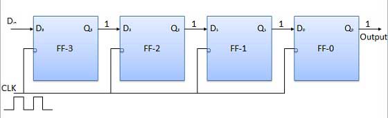
Similarly with Din = 1 and with the fourth negative clock edge arriving, the stored word in the register is Q3 Q2 Q1 Q0 = 1111.
Truth Table
Waveforms
Serial Input Parallel Output
- In such types of operations, the data is entered serially and taken out in parallel fashion.
- Data is loaded bit by bit. The outputs are disabled as long as the data is loading.
- As soon as the data loading gets completed, all the flip-flops contain their required data, the outputs are enabled so that all the loaded data is made available over all the output lines at the same time.
- 4 clock cycles are required to load a four bit word. Hence the speed of operation of SIPO mode is same as that of SISO mode.
Block Diagram
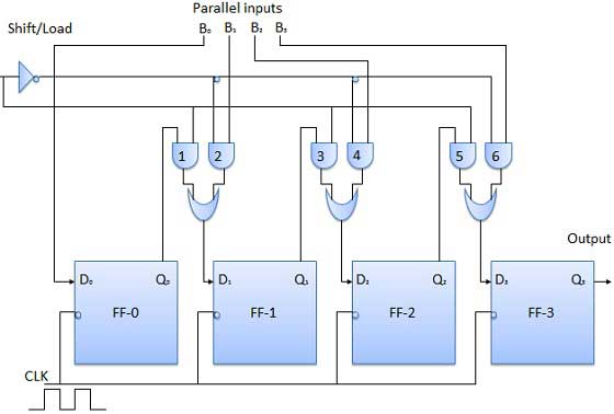
Parallel Input Serial Output (PISO)
- Data bits are entered in parallel fashion.
- The circuit shown below is a four bit parallel input serial output register.
- Output of previous Flip Flop is connected to the input of the next one via a combinational circuit.
- The binary input word B0, B1, B2, B3 is applied though the same combinational circuit.
- There are two modes in which this circuit can work namely – shift mode or load mode.
Load mode
When the shift/load bar line is low (0), the AND gate 2, 4 and 6 become active they will pass B1, B2, B3 bits to the corresponding flip-flops. On the low going edge of clock, the binary input B0, B1, B2, B3 will get loaded into the corresponding flip-flops. Thus parallel loading takes place.
Shift mode
When the shift/load bar line is low (1), the AND gate 2, 4 and 6 become inactive. Hence the parallel loading of the data becomes impossible. But the AND gate 1,3 and 5 become active. Therefore the shifting of data from left to right bit by bit on application of clock pulses. Thus the parallel in serial out operation takes place.
Block Diagram
Parallel Input Parallel Output (PIPO)
In this mode, the 4 bit binary input B0, B1, B2, B3 is applied to the data inputs D0, D1, D2, D3respectively of the four flip-flops. As soon as a negative clock edge is applied, the input binary bits will be loaded into the flip-flops simultaneously. The loaded bits will appear simultaneously to the output side. Only clock pulse is essential to load all the bits.
Block Diagram
Bidirectional Shift Register
- If a binary number is shifted left by one position then it is equivalent to multiplying the original number by 2. Similarly if a binary number is shifted right by one position then it is equivalent to dividing the original number by 2.
- Hence if we want to use the shift register to multiply and divide the given binary number, then we should be able to move the data in either left or right direction.
- Such a register is called bi-directional register. A four bit bi-directional shift register is shown in fig.
- There are two serial inputs namely the serial right shift data input DR, and the serial left shift data input DL along with a mode select input (M).
Block Diagram
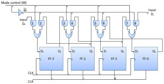
Operation
S.N.ConditionOperation1With M = 1 − Shift right operation
If M = 1, then the AND gates 1, 3, 5 and 7 are enabled whereas the remaining AND gates 2, 4, 6 and 8 will be disabled.
The data at DR is shifted to right bit by bit from FF-3 to FF-0 on the application of clock pulses. Thus with M = 1 we get the serial right shift operation.2With M = 0 − Shift left operation
When the mode control M is connected to 0 then the AND gates 2, 4, 6 and 8 are enabled while 1, 3, 5 and 7 are disabled.
The data at DL is shifted left bit by bit from FF-0 to FF-3 on the application of clock pulses. Thus with M = 0 we get the serial right shift operation.
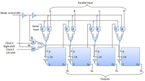
Universal Shift Register
A shift register which can shift the data in only one direction is called a uni-directional shift register. A shift register which can shift the data in both directions is called a bi-directional shift register. Applying the same logic, a shift register which can shift the data in both directions as well as load it parallely, is known as a universal shift register. The shift register is capable of performing the following operation −
- Parallel loading
- Left Shifting
- Right shifting
The mode control input is connected to logic 1 for parallel loading operation whereas it is connected to 0 for serial shifting. With mode control pin connected to ground, the universal shift register acts as a bi-directional register. For serial left operation, the input is applied to the serial input which goes to AND gate-1 shown in figure. Whereas for the shift right operation, the serial input is applied to D input.
Block Diagram
Digital Counters
Counter is a sequential circuit. A digital circuit which is used for a counting pulses is known counter. Counter is the widest application of flip-flops. It is a group of flip-flops with a clock signal applied. Counters are of two types.
- Asynchronous or ripple counters.
- Synchronous counters.
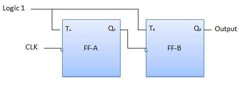
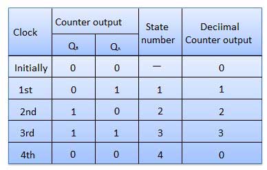
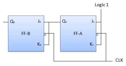
Asynchronous or ripple counters
The logic diagram of a 2-bit ripple up counter is shown in figure. The toggle (T) flip-flop are being used. But we can use the JK flip-flop also with J and K connected permanently to logic 1. External clock is applied to the clock input of flip-flop A and QA output is applied to the clock input of the next flip-flop i.e. FF-B.
Logical Diagram
Operation
S.N.ConditionOperation
1Initially let both the FFs be in the reset stateQBQA = 00 initially
2After 1st negative clock edge
As soon as the first negative clock edge is applied, FF-A will toggle and QA will be equal to 1.
QA is connected to clock input of FF-B. Since QAhas changed from 0 to 1, it is treated as the positive clock edge by FF-B. There is no change in QB because FF-B is a negative edge triggered FF.
QBQA = 01 after the first clock pulse.3After 2nd negative clock edge
On the arrival of second negative clock edge, FF-A toggles again and QA = 0.
The change in QA acts as a negative clock edge for FF-B. So it will also toggle, and QBwill be 1.
QBQA = 10 after the second clock pulse.4After 3rd negative clock edge
On the arrival of 3rd negative clock edge, FF-A toggles again and QAbecome 1 from 0.
Since this is a positive going change, FF-B does not respond to it and remains inactive. So QBdoes not change and continues to be equal to 1.
QBQA = 11 after the third clock pulse.5After 4th negative clock edge
On the arrival of 4th negative clock edge, FF-A toggles again and QAbecomes 1 from 0.
This negative change in QAacts as clock pulse for FF-B. Hence it toggles to change QBfrom 1 to 0.
QBQA = 00 after the fourth clock pulse.
Truth Table
Synchronous counters
If the “clock” pulses are applied to all the flip-flops in a counter simultaneously, then such a counter is called as synchronous counter.
2-bit Synchronous up counter
The JA and KA inputs of FF-A are tied to logic 1. So FF-A will work as a toggle flip-flop. The JB and KB inputs are connected to QA.
Logical Diagram
Operation
S.N.ConditionOperation1Initially let both the FFs be in the reset stateQBQA = 00 initially.2After 1st negative clock edge
As soon as the first negative clock edge is applied, FF-A will toggle and QA will change from 0 to 1.
But at the instant of application of negative clock edge, QA , JB = KB = 0. Hence FF-B will not change its state. So QBwill remain 0.
QBQA = 01 after the first clock pulse.3After 2nd negative clock edge
On the arrival of second negative clock edge, FF-A toggles again and QAchanges from 1 to 0.
But at this instant QA was 1. So JB = KB= 1 and FF-B will toggle. Hence QB changes from 0 to 1.
QBQA = 10 after the second clock pulse.4After 3rd negative clock edge
On application of the third falling clock edge, FF-A will toggle from 0 to 1 but there is no change of state for FF-B.
QBQA = 11 after the third clock pulse.5After 4th negative clock edge
On application of the next clock pulse, QAwill change from 1 to 0 as QB will also change from 1 to 0.
QBQA = 00 after the fourth clock pulse.
Classification of counters
Depending on the way in which the counting progresses, the synchronous or asynchronous counters are classified as follows −
- Up counters
- Down counters
- Up/Down counters
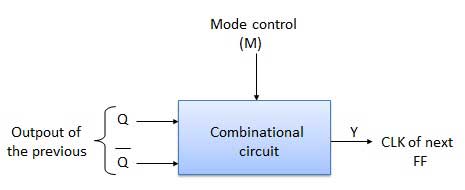
UP/DOWN Counter
Up counter and down counter is combined together to obtain an UP/DOWN counter. A mode control (M) input is also provided to select either up or down mode. A combinational circuit is required to be designed and used between each pair of flip-flop in order to achieve the up/down operation.
- Type of up/down counters
- UP/DOWN ripple counters
- UP/DOWN synchronous counter
UP/DOWN Ripple Counters
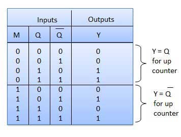
In the UP/DOWN ripple counter all the FFs operate in the toggle mode. So either T flip-flops or JK flip-flops are to be used. The LSB flip-flop receives clock directly. But the clock to every other FF is obtained from (Q = Q bar) output of the previous FF.
- UP counting mode (M=0) − The Q output of the preceding FF is connected to the clock of the next stage if up counting is to be achieved. For this mode, the mode select input M is at logic 0 (M=0).
- DOWN counting mode (M=1) − If M = 1, then the Q bar output of the preceding FF is connected to the next FF. This will operate the counter in the counting mode.
Example
3-bit binary up/down ripple counter.
- 3-bit − hence three FFs are required.
- UP/DOWN − So a mode control input is essential.
- For a ripple up counter, the Q output of preceding FF is connected to the clock input of the next one.
- For a ripple up counter, the Q output of preceding FF is connected to the clock input of the next one.
- For a ripple down counter, the Q bar output of preceding FF is connected to the clock input of the next one.
- Let the selection of Q and Q bar output of the preceding FF be controlled by the mode control input M such that, If M = 0, UP counting. So connect Q to CLK. If M = 1, DOWN counting. So connect Q bar to CLK.
Block Diagram
Truth Table
Operation
S.N.ConditionOperation1Case 1 − With M = 0 (Up counting mode)
If M = 0 and M bar = 1, then the AND gates 1 and 3 in fig. will be enabled whereas the AND gates 2 and 4 will be disabled.
Hence QA gets connected to the clock input of FF-B and QBgets connected to the clock input of FF-C.
These connections are same as those for the normal up counter. Thus with M = 0 the circuit work as an up counter.2Case 2: With M = 1 (Down counting mode)
If M = 1, then AND gates 2 and 4 in fig. are enabled whereas the AND gates 1 and 3 are disabled.
Hence QA bar gets connected to the clock input of FF-B and QBbar gets connected to the clock input of FF-C.
These connections will produce a down counter. Thus with M = 1 the circuit works as a down counter.
Modulus Counter (MOD-N Counter)
The 2-bit ripple counter is called as MOD-4 counter and 3-bit ripple counter is called as MOD-8 counter. So in general, an n-bit ripple counter is called as modulo-N counter. Where, MOD number = 2n.
Type of modulus
- 2-bit up or down (MOD-4)
- 3-bit up or down (MOD-8)
- 4-bit up or down (MOD-16)
Application of counters
- Frequency counters
- Digital clock
- Time measurement
- A to D converter
- Frequency divider circuits
- Digital triangular wave generator
